



Semiconductor Packaging: How the Back End Became a Strategic Choke Point
August 2026
Altman Solon is the largest global telecommunications, media, and technology consulting firm. In this insight, we examine how advanced packaging is changing the economics of semiconductor manufacturing and where that creates opportunity for operators and investors.
The economics of chipmaking are shifting from the front end to the back end. As Moore's Law, which posits that the number of transistors on a microchip doubles about every two years, hits physical and economic ceilings, monolithic chip designs are giving way to disaggregated chiplet and 3D-stacked architectures that depend on advanced packaging to integrate their components.
Demand for energy-efficient AI silicon is providing the scale to accelerate that shift. The most immediate implication is that packaging, once a back-end afterthought, has become a strategic choke point in the chip ecosystem. It now accounts for up to 20-30% of total AI chip manufacturing costs, and requires precision once reserved for the front-end, blurring the traditional line between the two. This "front-end-ization" of the back end marks a pivot from a low-capital, commodity activity to an advanced domain with strong growth and margins approaching front-end levels.
The advanced back end takes center stage
Historically, the semiconductor front end (wafer fab) and back end (slicing, testing, and packaging) were separate worlds. The back end was the lower-value step: commoditized, labor-intensive work that connected package pins to die bumps and protected the die. While IDMs retained significant in-house assembly and test operations, U.S. semiconductor manufacturers began shifting parts of this labor-intensive work to East and Southeast Asia from the 1960s — initially often through captive offshore facilities and increasingly through specialist subcontractors.
Companies such as Amkor, ASE, and JCET scaled the outsourced segment into a multi-billion-dollar industry that stayed cost-oriented relative to the front end.
That is changing. For decades, performance gains came from transistor scaling, but over the past five years, the physical and economic limits of Moore's Law have become clear. As miniaturization becomes more costly, and large monolithic dies face yield and reticle constraints, the industry is turning to chiplet-based architectures, integrating multiple smaller dies into one system through advanced packaging such as 2.5D/3D stacking. At the same time, generative AI and high-performance computing (HPC) workloads are placing intense demands on data movement, power efficiency, and memory bandwidth.
As front-end scaling becomes harder, performance gains are increasingly shifting toward system-level integration
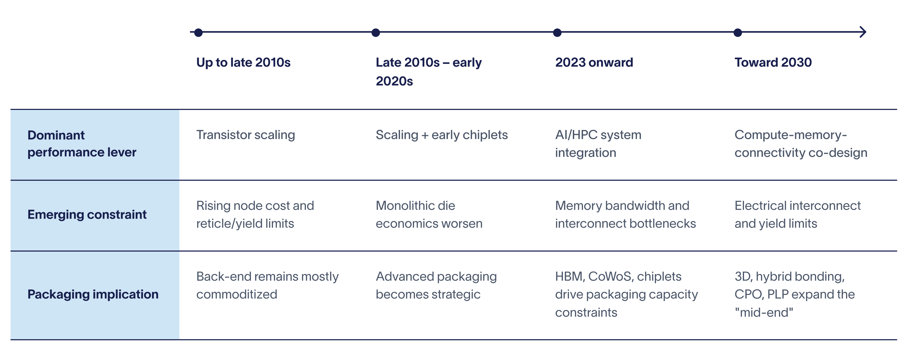
How HBM and chiplets are turning the back end into a battleground
Front-end scaling is becoming more expensive and hitting physical limits. When Moore's Law began to slow, made structurally obvious by the 7nm node in 2018, chipmakers turned to advanced packaging to keep performance improving.
Rather than chasing ever more expensive 3nm chips, companies began combining several cheaper 7nm chips in a single package, as AMD does in its EPYC server processors. Placing components closer together through 2.5D/3D stacking shortens the signal travel path, increasing speed and reducing power consumption without requiring smaller transistors.
Heterogeneous integration extends the logic: instead of one expensive chip, a package combines chiplets, using leading-edge nodes only where they earn their cost [e.g., 3nm for logic, mature 5nm or 7nm for SRAM (cache)]. Chiplets also improve effective yield, since a defect kills one small component rather than an entire monolithic die.
AI accelerators add a second driver: they require high-bandwidth memory (HBM); stacks of DRAM dies mounted next to the processor and joined through advanced methods such as hybrid bonding. Modern AI GPUs need more transistors than a single die can hold, so multiple dies are packaged together. HBM stacks are moving from today's 8- and 12-layer standards toward 16, 20, and 24 layers, with the tallest stacks already on SK Hynix’s and Samsung’s roadmaps for HBM4E after 2027.
While HBM addresses the data movement bottleneck between compute and memory within the package, the next constraint lies in efficiently moving data across the links between processors, accelerators, and networking components. Co-packaged optics extends the integration logic beyond the package to these system-level connections, broadening advanced packaging’s role from chip integration to system-level connectivity.
Together, HBM and chiplets (and over time, CPO) are driving the growth in advanced packaging.
Advanced packaging is a growth opportunity for equipment makers
The rapid adoption of HBM, chiplets, and heterogeneous integration is driving heavy investment in advanced packaging capacity by OSATs, foundries, and IDMs, and that is expanding the market for back-end equipment. The market is expected to grow from about $12.6 billion in 2024 to $29.4 billion by 2028, a compound annual growth rate near 24%. Importantly, this growth is not just volume-driven: increasing device complexity is raising the value per process step and increasing equipment spend per chip.
Leading-edge packaging tools now command gross margins comparable to front-end equipment: roughly 60-65% for hybrid bonding and high-end HBM tools, 40-50% for 2.5D/3D packaging, and 50-60% for metrology and inspection. The economic center of gravity in the equipment market is moving toward the back end.
Advanced packaging increasingly requires the same high-precision tools and process technologies that were previously reserved for front-end wafer fabrication. To enable advanced packaging architectures such as 2.5D/3D integration, chiplets, and HBM, a new set of capabilities is required across the back end. These create the "mid-end," a zone where front end and back end converge, and it hands front-end equipment makers a natural adjacency to expand into.
What this means for operators and investors
Investors: The equipment layer is where the packaging boom converts into durable margins. Back-end tools re-rating toward front-end economics makes this the pick-and-shovel exposure to the AI build-out.
Equipment OEMs and packaging operators: The mid-end is contested ground. Front-end OEMs have a real opening to expand into packaging, and back-end specialists have to decide fast whether to defend through R&D, partner, or be outflanked. For equipment buyers, tool choice is now a performance decision, not just a cost one.
The semiconductor back end has moved from a commoditized afterthought to a strategic control point, in capacity, in margins, and now in the equipment that makes it possible. The companies that recognize it early, as investors or operators, will shape the next phase of the AI hardware value chain.
How Altman Solon can help
Altman Solon works across the semiconductor and hardware value chain, from chip design to device distribution, where capital intensity and technological complexity make every strategic decision consequential. In advanced packaging specifically, that work includes:
- Investor support: diligence, market theses, and screening across the packaging and back-end equipment value chain.
- Supply chain and operations: advising on fab investments, OSAT partnerships, and coordination of global design and manufacturing ecosystems.
- Product and go-to-market strategy: prioritizing roadmaps and launching effectively in categories where performance, not cost, now decides the sale.
- Model transitions: supporting shifts toward software-linked and recurring-revenue models aligned with customer and investor priorities.


Insights
Insights | August 2026
Insights | August 2026